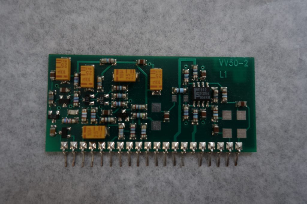
VV50 is a discrete charge sensitive pre-amplifier with configurable peaking time and gain. It is designed for negative input signals whereas the output signal polarity may be configured. Input and output are AC coupled. The core amplifier circuit comprises the fast cascode of a JFET in drain configuration and a bipolar transistor in base configuration. A successive fast video driver chip serves as gain booster and 50 Ohm line driver.
VV50 is a robust device for single channel radiation detection applications of counting type. It has proven very convenient for detector development in fields where individual elementary interactions are to be detected.
The gain may be configured between 0,1 mV/fC and 15mV/fC. Maximum output amplitude is 400mV. The ENC of the circuit amounts to ~ 600 el rms at low input capacitance of a few 10 pF. Peaking time can be configured between 100ns and ~1µs.
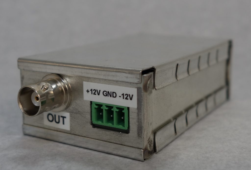
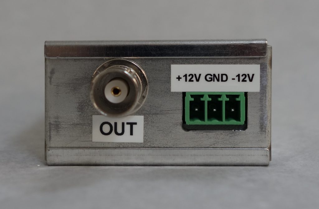
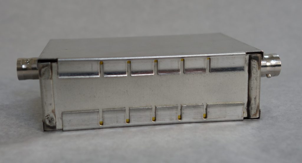
Input and output connectors are BNC.
The circuit needs a supply voltage of + 12V and -12V.
The circuit was developed by R. Rusnyak, Physikalisches Institut, Universität Heidelberg, 15.7.1995. It has been licenced by CDT GmbH.
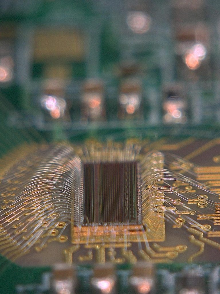
CDT has designed the detectors for neutron instrumentation around the 64 channel charge sensitive readout ASIC CIPix 1.1 designed and developed at the ASIC laboratory of Universität Heidelberg. The pre-amplifier and shaper circuitry was developed by Dr. Ulrich Trunk for the HELIX chip and later transfered to the CIPix.
The CIPix comprises 64 analogue readout channels where the signal of each terminates in a discriminator. The state of each discriminator is read out at a sampling frequency of 10 MHz. For diagnostic purposes the analogue signal of any individual single channel may be switched to one diagnostic analogue output buffer for observation on an ADC or oscilloscope.
The gain of the amplifiers is ~ 0,34 mV/fC at a peaking time of ~ 150 ns with a thermal noise performance of (380 e- + 38 e-/pF * Cin).
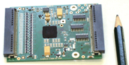
The CMOS chip has been integrated by CDT into the readout board AS20 which is available in various different configurations concerning interfacing connectors and data rates.
CDT has licenced the right for production and commercial use of the CIPix from University Heidelberg.